


News


 电商部
电商部  2026-01-26 10:31:20
 Core technology of wide-temperature solid-state drive: How to achieve stable operation in extreme te
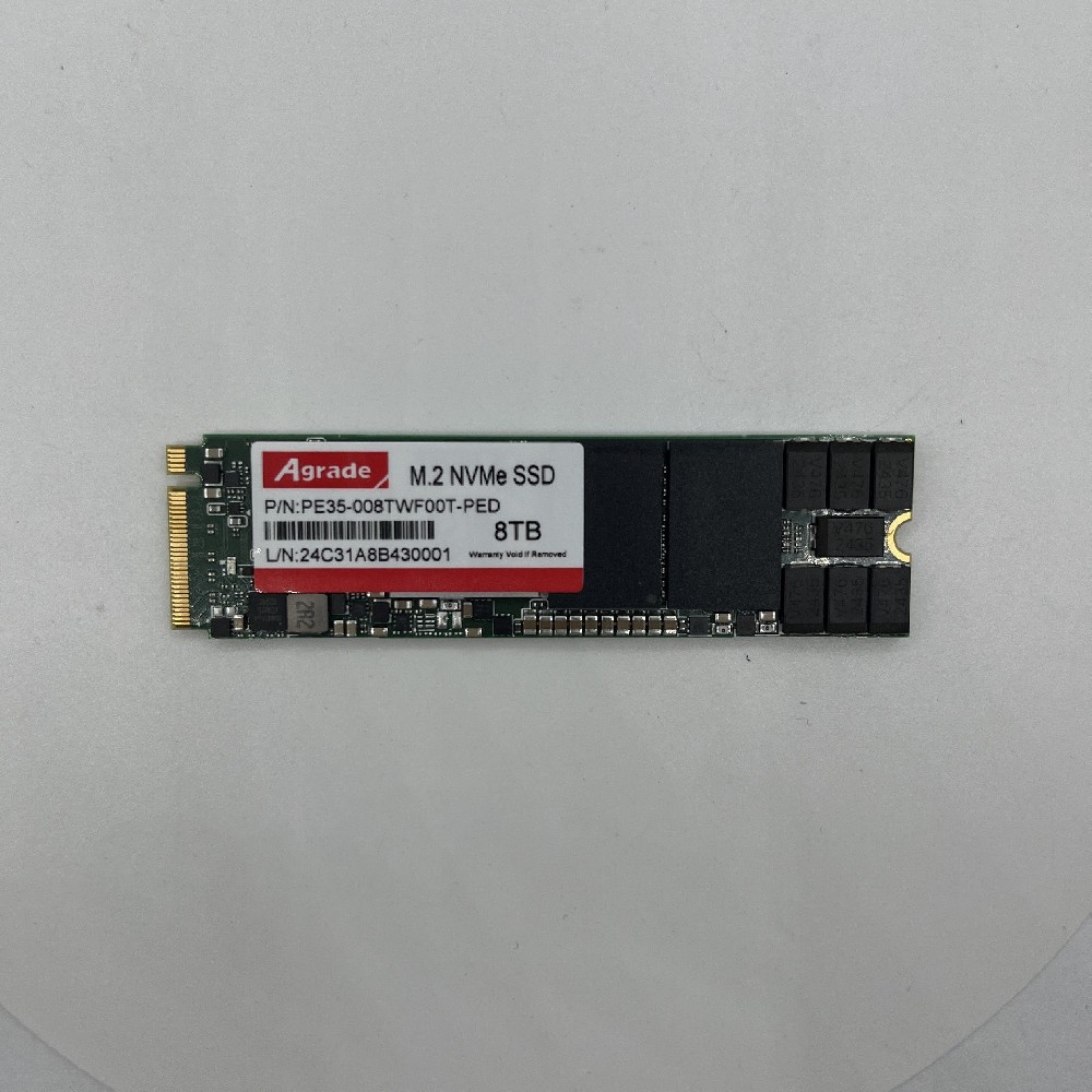
The reason why wide-temperature solid-state drives (SSDs) can break through the temperature limitations of ordinary SSDs and operate stably in extreme temperature ranges lies primarily in the collaborative optimization design at the chip, firmware, and hardware levels. For every 10°C expansion towards the edge of the temperature range, the design difficulty, device cost, and testing cycle all increase exponentially. It requires solving a series of technical challenges such as changes in device characteristics, degradation of signal integrity, and attenuation of data retention capability under high and low temperature environments, and building a full-chain temperature adaptability and reliability assurance system.

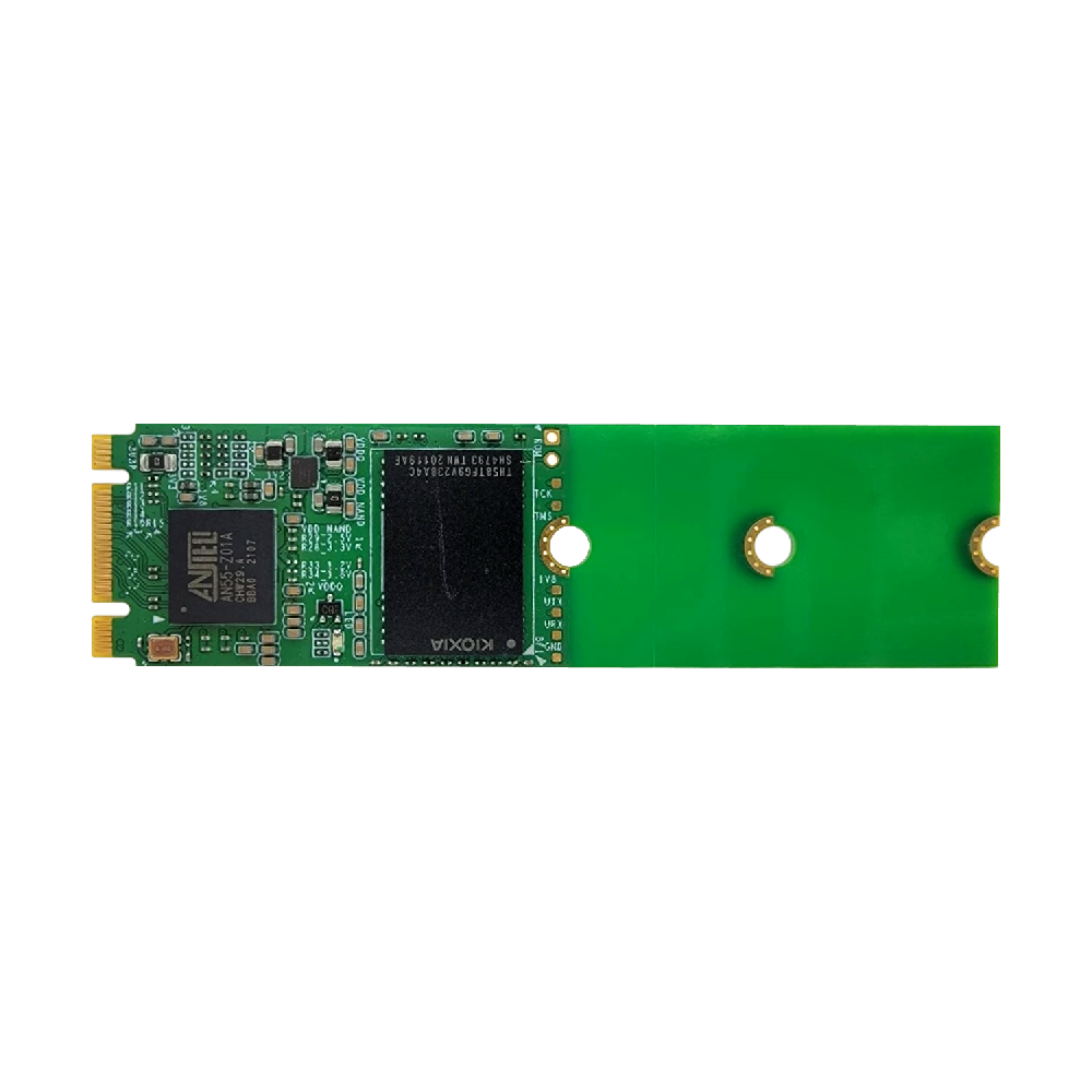
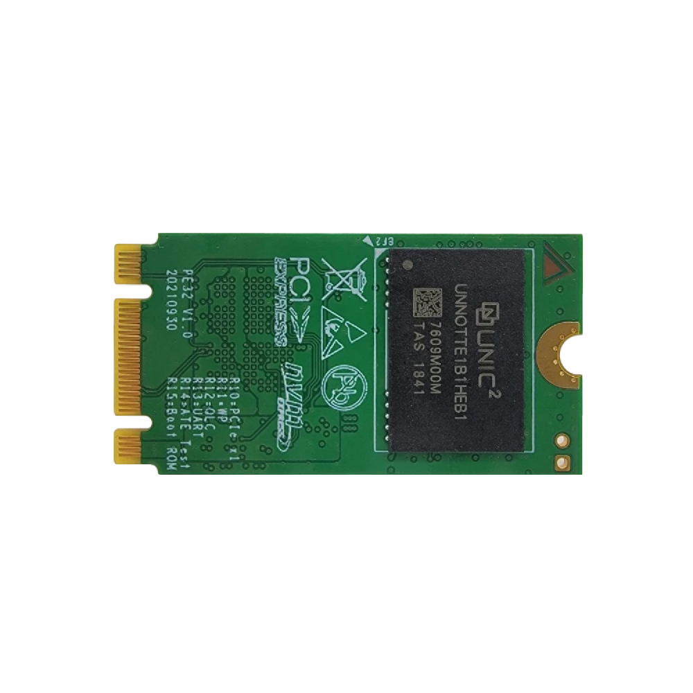
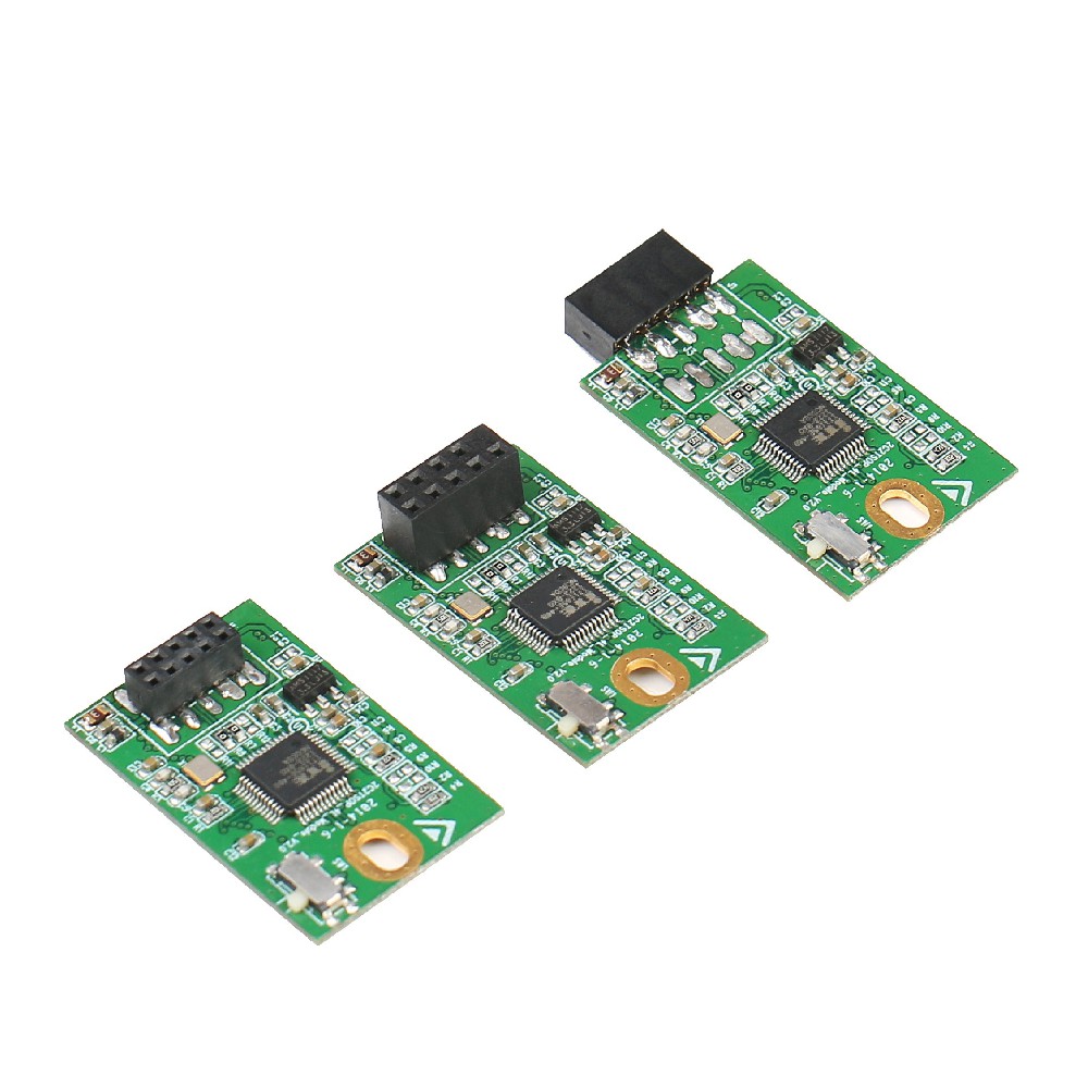
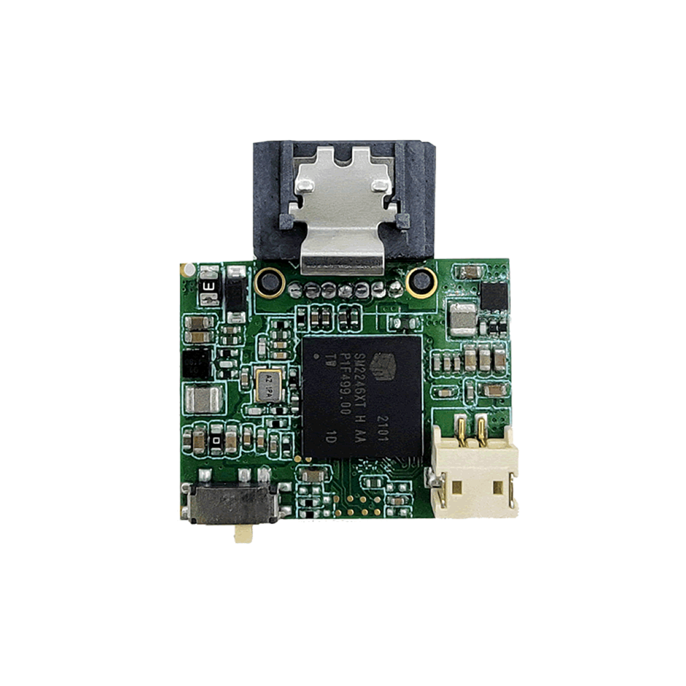
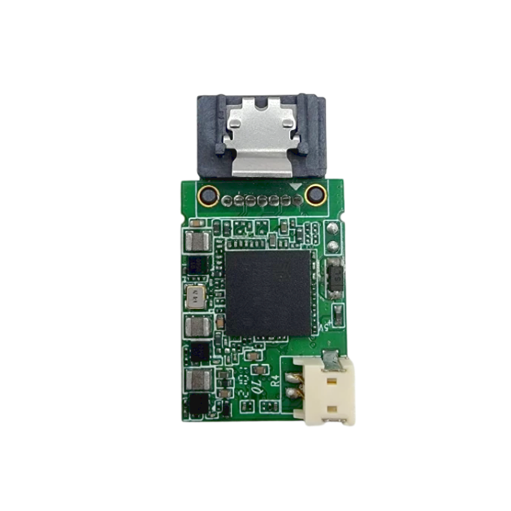
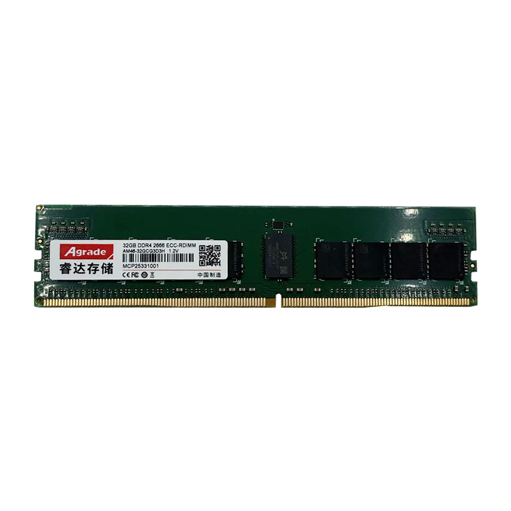
The chip level serves as the foundation for wide-temperature SSDs to achieve temperature adaptation, and the selection of components directly determines the upper temperature limit and operational stability. Manufacturers need to select NAND flash memories and controller chips with wide-temperature characteristics from the source, giving priority to components that have been certified by industrial and military standards such as AEC-Q100 and GJB150A. These chips have undergone thousands of temperature cycle tests and high and low temperature aging tests before leaving the factory, and can withstand extreme temperature differences ranging from -55℃ to 125℃. In low temperature environments, the electron mobility rate of flash memory cells decreases, and the write threshold voltage increases, making them prone to write failures or data errors. The controller chip needs to have stronger timing fault tolerance and voltage calibration capabilities, ensuring accurate data writing by optimizing the programming pulse width and voltage gradient. In high temperature environments, the charge leakage rate of flash memory cells accelerates, significantly reducing data retention capability. It is necessary to optimize the flash programming algorithm and data refresh mechanism to suppress the increase in bit error rate caused by charge leakage. Some high-end wide-temperature products also integrate high-precision temperature sensors to collect chip temperature data in real time, providing accurate basis for firmware regulation.
Firmware and hardware design form a dual safeguard, further enhancing temperature adaptability and operational stability. At the firmware level, algorithms such as dynamic voltage scaling, intelligent wear leveling, and temperature-adaptive read-write strategies are employed to adapt in real-time to fluctuations in flash memory characteristics caused by temperature changes. For instance, at high temperatures, read-write frequencies are reduced and power consumption allocation is optimized. At low temperatures, the boot voltage is increased and the warm-up time is extended, ensuring a balance between performance and reliability across different temperature ranges. In terms of hardware design, high thermal conductivity materials and optimized PCB layouts are utilized, concentrating heat-generating core components such as the controller and flash memory, paired with metal heat sinks or thermal conductive silicone gel to accelerate heat conduction. Some high-end products also feature active cooling mechanisms, achieving hierarchical power consumption control through dynamic frequency scaling in firmware. When the temperature approaches the warning threshold, the system gradually slows down, and once the temperature drops, performance is restored, forming a thermal throttling steady state. Additionally, the hardware power supply circuit adopts a wide voltage design and a tantalum capacitor energy storage module to avoid power supply instability caused by temperature fluctuations. This integrated system design of controller-firmware-structure enables wide-temperature SSDs to maintain stable performance and data security in extreme temperature ranges.
At the chip level, it is necessary to select NAND flash memory and main control chips with wide temperature characteristics, and verify the stability of the devices through rigorous temperature cycling tests. In low temperature environments, the write threshold of flash memory increases, and the main control needs to have stronger timing fault tolerance; at high temperatures, data retention capacity decreases, and flash programming algorithms need to be optimized to suppress charge leakage. Some high-end products also integrate temperature sensors to provide real-time feedback on environmental conditions.
Firmware and hardware design form a dual safeguard: firmware adapts to the fluctuations in flash memory characteristics caused by temperature changes through dynamic voltage scaling and wear leveling optimization; hardware employs high thermal conductivity materials and optimized PCB layout, and some products are equipped with active cooling mechanisms to achieve temperature closed-loop control under high loads. This system-level design enables wide-temperature SSDs to maintain stable performance and data security in extreme temperature ranges.

-
Products
Advantages
-
Solutions
-
News
About us
-
Contact us
Tel:+86 19926658803
Whatsapp:+86 19926658803
lianle1210@163.com
Address: 30CF, Caihong Building, Caihong Road, Futian District, Shenzhen City, Guangdong Province, China


Friendly Links:
